Background
Light-emitting diodes (LEDs)—small colored lights available in any electronics store—are ubiquitous in modern society. They are the indicator lights on our stereos, automobile dashboards, and microwave ovens. Numeric displays on clock radios, digital watches, and calculators are composed of bars of LEDs. LEDs also find applications in telecommunications for short range optical signal transmission such as TV remote controls. They have even found their way into jewelry and clothing—witness sun visors with a series of blinking colored lights adorning the brim. The inventors of the LED had no idea of the revolutionary item they were creating. They were trying to make lasers, but on the way they discovered a substitute for the light bulb.
Light bulbs are really just wires attached to a source of energy. They emit light because the wire heats up and gives off some of its heat energy in the form of light. An LED, on the other hand, emits light by electronic excitation rather than heat generation. Diodes are electrical valves that allow electrical current to flow in only one direction, just as a one-way valve might in a water pipe. When the valve is “on,” electrons move from a region of high electronic density to a region of low electronic density. This movement of electrons is accompanied by the emission of light. The more electrons that get passed across the boundary between layers, known as a junction, the brighter the light. This phenomenon, known as electroluminescence, was observed as early as 1907. Before working LEDs could be made, however, cleaner and more efficient materials had to be developed.
LEDs were developed during the post-World War II era; during the war there was a potent interest in materials for light and microwave detectors. A variety of semiconductor materials were developed during this research effort, and their light interaction properties were investigated in some detail. During the 1950s, it became clear that the same materials that were used to detect light could also be used to generate light. Researchers at AT&T Bell Laboratories were the first to exploit the light-generating properties of these new materials in the 1960s. The LED was a forerunner, and a fortuitous byproduct, of the laser development effort. The tiny colored lights held some interest for industry, because they had advantages over light bulbs of a similar size: LEDs use less power, have longer lifetimes, produce little heat, and emit colored light.
The first LEDs were not as reliable or as useful as those sold today. Frequently, they could only operate at the temperature of liquid nitrogen (-104 degrees Fahrenheit or -77 degrees Celsius) or below, and would bum out in only a few hours. They gobbled power because they were very inefficient, and they produced very little light. All of these problems can be attributed to a lack of reliable techniques for producing the appropriate materials in the 1950s and 1960s, and as a result the devices made from them were poor. When materials were improved, other advances in the technology followed: methods for connecting the devices electronically, enlarging the diodes, making them brighter, and generating more colors.
The advantages of the LED over the light bulb for applications requiring a small light source encouraged manufacturers like Texas Instruments and Hewlett Packard to pursue the commercial manufacture of LEDs. Sudden widespread market acceptance in the 1970s was the result of the reduction in production costs and also of clever marketing, which made products with LED displays (such as watches) seem “high tech” and, therefore, desirable. Manufacturers were able to produce many LEDs in a row to create a variety of displays for use on clocks, scientific instruments, and computer card readers. The technology is still developing today as manufacturers seek ways to make the devices more efficiently, less expensively, and in more colors.
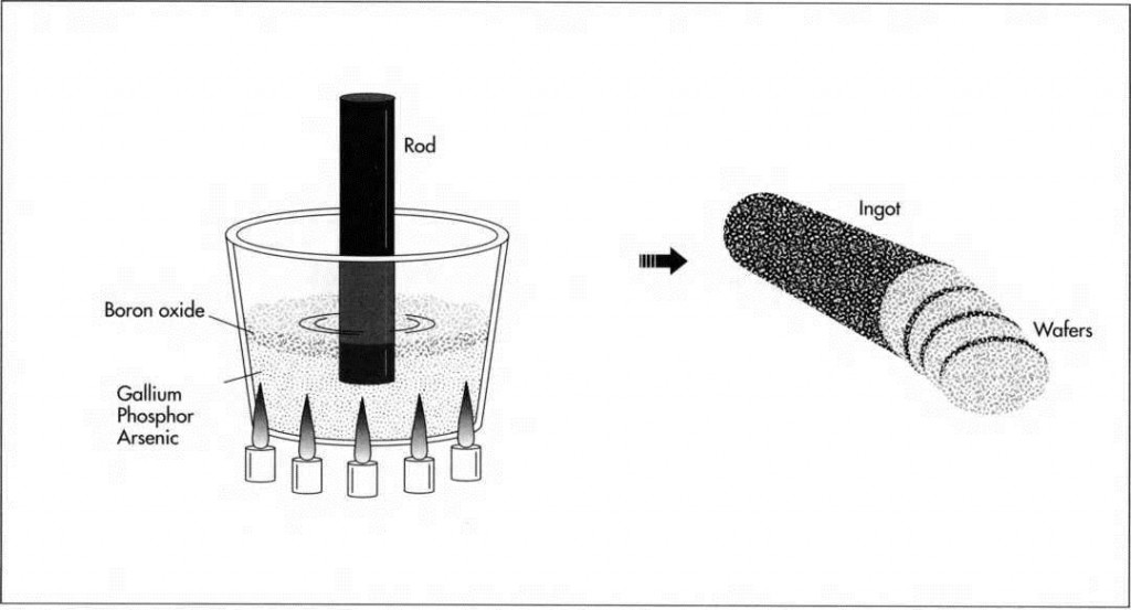
(To make the semiconductor wafers, gallium, arsenic, and/or phosphor are first mixed together in a chamber and forced into a solution. To keep them from escaping into the pressurized gas in the chamber, they are often covered with a layer of liquid boron oxide. Next, a rod is dipped into the solution and pulled out slowly. The solution cools and crystallizes on the end of the rod as it is lifted out of the chamber, forming a long, cylindrical crystal ingot. The ingot is then sliced into wafers.)
Raw Materials
Diodes, in general, are made of very thin layers of semiconductor material; one layer will have an excess of electrons, while the next will have a deficit of electrons. This difference causes electrons to move from one layer to another, thereby generating light. Manufacturers can now make these layers as thin as .5 micron or less (1 micron = 1 ten-thousandth of an inch).
Impurities within the semiconductor are used to create the required electron density. A semiconductor is a crystalline material that conducts electricity only when there is a high density of impurities in it. The slice, or wafer, of semiconductor is a single uniform crystal, and the impurities are introduced later during the manufacturing process. Think of the wafer as a cake that is mixed and baked in a prescribed manner, and impurities as nuts suspended in the cake. The particular semiconductors used for LED manufacture are gallium arsenide (GaAs), gallium phosphide (GaP), or gallium arsenide phosphide (GaAsP). The different semiconductor materials (called substrates) and different impurities result in different colors of light from the LED.
Impurities, the nuts in the cake, are introduced later in the manufacturing process; unlike imperfections, they are introduced deliberately to make the LED function correctly. This process is called doping. The impurities commonly added are zinc or nitro-gen, but silicon, germanium, and tellurium have also been used. As mentioned previously, they will cause the semiconductor to conduct electricity and will make the LED function as an electronic device. It is through the impurities that a layer with an excess or a deficit of electrons can be created.
To complete the device, it is necessary to bring electricity to it and from it. Thus, wires must be attached onto the substrate. These wires must stick well to the semiconductor and be strong enough to withstand subsequent processing such as soldering and heating. Gold and silver compounds are most commonly used for this purpose, because they form a chemical bond with the gallium at the surface of the wafer.
LEDs are encased in transparent plastic, rather like the lucite paperweights that have objects suspended in them. The plastic can be any of a number of varieties, and its exact optical properties will determine what the output of the LED looks like. Some plastics are diffusive, which means the light will scatter in many directions. Some are transparent, and can be shaped into lenses that will direct the light straight out from the LED in a narrow beam. The plastics can be tinted, which will change the color of the LED by allowing more or less of light of a particular color to pass through.
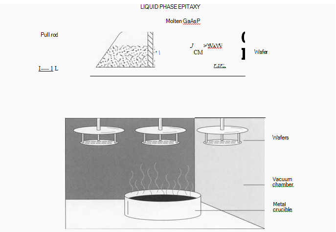
(One way to add the necessary impurities to the semiconductor crystal is to grow additional layers of crystal onto the wafer surface. In this process, known as “Liquid Phase Epitaxy,” the wafer is put on a graphite slide and passed underneath reservoirs of molten GaAsP. Contact patterns are exposed on the wafer’s surface using photoresist, after which the wafers are put into a heated vacuum chamber. Here, molten metal is evaporated onto the contact pattern on die wafer surface.)
Design
Several features of the LED need to be considered in its design, since it is both an electronic and an optic device. Desirable optical properties such as color, brightness, and efficiency must be optimized without an unreasonable electrical or physical design. These properties are affected by the size of the diode, the exact semiconductor materials used to make it, the thickness of the diode layers, and the type and amount of impurities used to “dope” the semiconductor.
The Manufacturing Process
Making semiconductor wafers
1 First, a semiconductor wafer is made. The particular material composition—GaAs GaP, or something in between—is determined by the color of LED being fabricated. The crystalline semiconductor is grown in a high temperature, high pressure chamber. Gallium, arsenic, and/or phosphor are purified and mixed together in the chamber. The heat and pressure liquify and press the components together so that they are forced into a solution. To keep them from escaping into the pressurized gas in the chamber, they are often covered with a layer of liquid boron oxide, which seals them off so that they must “stick together.” This is known as liquid encapsulation, or the Czochralski crystal growth method. After the elements are mixed in a uniform solution, a rod is dipped into the solution and pulled out slowly. The solution cools and crystallizes on the end of the rod as it is lifted out of the chamber, forming a long, cylindrical crystal ingot (or boule) of GaAs, GaP, or GaAsP. Think of this as baking the cake.
2 The boule is then sliced into very thin wafers of semiconductor, approximately 1mils thick, or about as thick as a garbage bag. The wafers are polished until the surfaces are very smooth, so that they will readily accept more layers of semiconductor on their surface. The principle is similar to sanding a table before painting it. Each wafer should be a single crystal of material of uniform composition. Unfortunately, there will sometimes be imperfections in the crystals that make the LED function poorly. Think of imperfections as unmixed bits of flower or sugar suspended in the cake during baking. Imperfections can also result from the polishing process; such imperfections also degrade device performance. The more imperfections, the less the wafer behaves like a single crystal; without a regular crystalline structure, the material will not function as a semiconductor.
3 Next, the wafers are cleaned through a rigorous chemical and ultrasonic process using various solvents. This process removes dirt, dust, or organic matter that may have settled on the polished wafer surface. The cleaner the processing, the better the resulting LED will be.
Adding epitaxial layers
4 Additional layers of semiconductor crystal are grown on the surface of the wafer, like adding more layers to the cake. This is one way to add impurities, or dopants, to the crystal. The crystal layers are grown this time by a process called Liquid Phase Epitaxy (LPE). In this technique, epitaxial layers—semiconductor layers that have the same crystalline orientation as the substrate below—are deposited on a wafer while it is drawn under reservoirs of molten GaAsP. The reservoirs have appropriate dopants mixed through them. The wafer rests on a graphite slide, which is pushed through a channel under a container holding the molten liquid (or melt, as it is called). Different dopants can be added in sequential melts, or several in the same melt, creating layers of material with different electronic densities. The deposited layers will become a continuation of the wafer’s crystal structure.
LPE creates an exceptionally uniform layer of material, which makes it a preferred growth and doping technique. The layers formed are several microns thick.
5 After depositing epitaxial layers, it may be necessary to add additional dopants to alter the characteristics of the diode for color or efficiency. If additional doping is done, the wafer is again placed in a high temperature furnace tube, where it is immersed in a gaseous atmosphere containing the dopants—nitrogen or zinc ammonium are the most common. Nitrogen is often added to the top layer of the diode to make the light more yellow or green.
Adding metal contacts
6 Metal contacts are then defined on the wafer. The contact pattern is determined in the design stage and depends on whether the diodes are to be used singly or in combination. Contact patterns are reproduced in photoresist, a light-sensitive compound; the liquid resist is deposited in drops while the wafer spins, distributing it over the surface. The resist is hardened by a brief, low temperature baking (about 215 degrees Fahrenheit or 100 degrees Celsius). Next, the master pattern, or mask, is duplicated on the photoresist by placing it over the wafer and exposing the resist with ultraviolet light (the same way a photograph is made from a negative). Exposed areas of the resist are washed away with developer, and unexposed areas remain, covering the semiconductor layers.
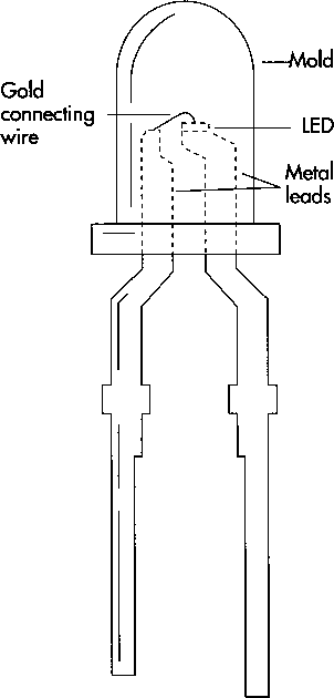
(A typical LED indicator light shows how small the actual LED is. Although the average lifetime of a small light bulb is 5-10 years, a modem LED should last 100 years or more before it fails.)
Contact metal is now evaporated onto the pattern, filling in the exposed areas. Evaporation takes place in another high temperature chamber, this time vacuum sealed. A chunk of metal is heated to temperatures that cause it to vaporize. It condenses and sticks to the exposed semiconductor wafer, much like steam will fog a cold window. The photoresist can then be washed away with acetone, leaving only the metal contacts behind. Depending on the final mounting scheme for the LED, an additional layer of metal may be evaporated on the back side of the wafer. Any deposited metal must undergo an annealing process, in which the wafer is heated to several hundred degrees and allowed to remain in a furnace (with an inert atmosphere of hydrogen or nitrogen flowing through it) for periods up to several hours. During this time, the metal and the semiconductor bond together chemically so the contacts don’t flake off.
8 A single 2 inch-diameter wafer produced in this manner will have the same pattern repeated up to 6000 times on it; this gives an indication of the size of the finished diodes. The diodes are cut apart either by cleaving (snapping the wafer along a crystal plane) or by sawing with a diamond saw. Each small segment cut from the wafer is called a die. A difficult and error prone process, cutting results in far less than 6000 total useable LEDs and is one of the biggest challenges in limiting production costs of semiconductor devices.
Mounting and packaging
9 Individual dies are mounted on the appropriate package. If the diode will be used by itself as an indicator light or for jewelry, for example, it is mounted on two metal leads about two inches long. Usually, in this case, the back of the wafer is coated with metal and forms an electrical contact with the lead it rests on. A tiny gold wire is soldered to the other lead and wire-bonded to the patterned contacts on the surface of the die. In wire bonding, the end of the wire is pressed down on the contact metal with a very fine needle. The gold is soft enough to deform and stick to a like metal surface. Finally, the entire assembly is sealed in plastic. The wires and die are suspended inside a mold that is shaped according to the optical requirements of the package (with a lens or connector at the end), and the mold is filled with liquid plastic or epoxy. The epoxy is cured, and the package is complete.
Quality Control
Quality in semiconductor manufacturing takes two forms. The first concern is with the final produced product, and the second with the manufacturing facility. Every LED is checked when it is wire bonded for operation characteristics. Specific levels of current should produce specific brightness. Exact light color is tested for each batch of wafers, and some LEDs will be pulled for stress testing, including lifetime tests, heat and power breakdown, and mechanical damage.
In order to produce products consistently, the manufacturing line has to operate reliably and safely. Many of the processing steps above can be automated, but not all are. The general cleanliness of the facility and incoming blank wafers is monitored closely. Special facilities (“clean rooms”) are built that keep the air pure up to one part in 10,000 for particular processing steps (particularly numbers 1-5 above). All of these checks arise from a desire to improve the yield, or the number of successful LEDs per wafer.
The Future
Optoelectronics is blossoming with the advent of better and better processing techniques. It is now possible to make wafers with a purity and uniformity unheard of 5 years ago. This will effect how bright and how efficient LEDs can be made, and how long they will last. As they get better, they are appropriate for increasingly demanding applications, such as communications. The average lifetime of a small light bulb is 5-10 years, but the average modem LED should last 100 years before failure. This makes them suitable for applications where it is difficult or impossible to replace parts, such as undersea or outerspace electronics. Although LEDs are inappropriate for long-range optical fiber transmission, they are often useful for short range optical transmission such as remote controls, chip to chip communication, or excitation of optical amplifiers.
Other materials are being developed that will allow fabrication of blue and white light LEDs. In addition to making possible a wider variety of indicators and toys with more colors, blue light is preferable for some applications such as optical storage and visual displays. Blue and white light are easier on the eyes. Additional colors would certainly open up new applications.
Finally, as process technology advances and it becomes possible to incorporate more devices on a single chip, LED displays will become more “intelligent.” A single microchip will hold all the electronics to create an alphanumeric display, and will make instrumentation smaller and more sophisticated.
Where To Learn More
Books
Bergh, A. A. and p. J Dean. Light-Emitting Diodes. Clarendon Press, 1976.
Gillessen, Klaus. Light-Emitting Diodes: An Introduction. Prentice Hall, 1987.
Optoelectronics/Fiber-Optics Applications Manual. McGraw-Hill, 1981.
Understanding Solid State Electronics. Radio Shack/Texas Instruments Learning Center, 1978.
Williams, E. w. and R. Hall. Luminescence and the Light-Emitting Diode. Pergamon Press, 1978.
Periodicals
Cole, Bernard c. “Now a LED Can Take On the Light Bulb.” Electronics. October, 1988, p. 41.
Iversen, Wesley R. “Would You Believe LED Brake Lights.” Electronics. September 18, 1986.
Marston, Ray. “Working with LED’s.” Radio-Electronics. January, 1992, p. 50; February, 1992, p. 69.
Weisburd, Stefi. “Silicon Devices: LED There Be Light.” Science News. May 9,
1987, p. 294

